- Need Free Consultation ?

Get Consultation
Liam@hengele.com Sale@hengele.com
Circuit Board Testing and Quality Assurance
Inspection and testing are critical aspects of getting your products to market. Persistent failures or recalls can cause not only financial losses, but also irreparable damage to your reputation for quality. That’s why it’s critical to work with a PCB manufacturer that offers comprehensive board testing.
At EMSG, we know that quality control cannot be compromised. As a full-service provider of turnkey board testing solutions, we’ll work with you to find the optimal solution for testing your product while maintaining acceptable cycle times.
Read on to learn more about the technical details of our optical inspection, functional testing and in-circuit PCB testing services, as well as our broader commitment to quality assurance. We are happy to answer any questions you may have by phone or email, or to arrange a face-to-face consultation at your convenience.
Customer Service
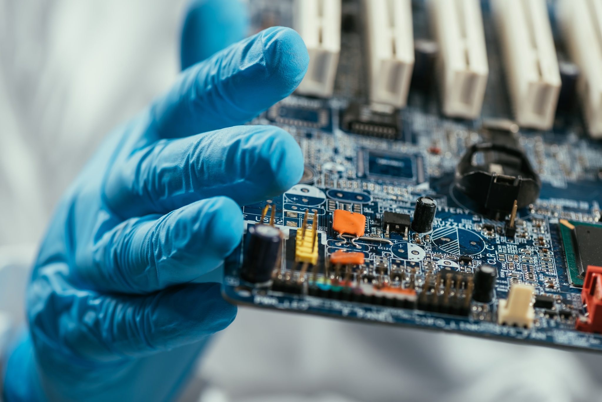
Different types of electronic products often require customised inspection processes before they leave the factory. Hentech visually inspects each product at 100% magnification to ensure that it meets the customer’s technical requirements and quality standards. In addition, we offer a wide range of inspection services to ensure that all products delivered are fully compliant with individual customer specifications.
Depending on the quantity and complexity of the product, we are equipped with an Automated Optical Inspection (AOI) system that effectively identifies common problems at the component level, such as incorrectly orientated mounting, missing, damaged or incorrectly assembled components. The system also detects defective solder joints as small as 12 mils apart, including common soldering issues such as bridging and solder fill.
Hentech offers in-line AOI inspection services when the project requirements include electrical inspection. We also support the use of customer-supplied test equipment or customised functional test platforms, depending on the project requirements, to ensure the reliability and stability of the product in the final application.
Efficient and reliable PCB design and assembly process
Ensuring consistent performance and reliable quality in printed circuit board (PCB) manufacturing is at the heart of what we do. Visual inspections alone can make it difficult to detect all potential problems, so we pay attention to every manufacturing detail to improve product consistency and reliability.
At Hentech, we emphasise efficient production and uncompromising quality. We know that our customers can’t afford the delays and costs associated with rework, so we’re committed to assembling quality products that meet design requirements and always do it right the first time.
While our placement equipment can place up to 40,000 components per hour, we maintain quality control throughout the production process to ensure that reliability is not sacrificed for efficiency.
From initial prototyping and parts sourcing to precision assembly, inspection, and functional testing, Hentech implements rigorous quality management processes at every step of the process to ensure that every board delivered meets or exceeds our customers’ technical standards.
Take an in-depth look at our PCB assembly process and learn how each step of the process contributes to a high quality end product.
Prototyping/Customization
Before launching formal production, we will assist in the production of PCB prototypes based on customers’ customization requirements. Through prototyping, potential problems in component layout and assembly can be identified and solved in advance, effectively saving time and cost in mass production.
Our team of engineers will also help you choose the most appropriate assembly process. We have the equipment to handle both Surface Mount (SMT) and Through Hole Threading (THT) assembly methods. Surface mounting involves mounting components on the surface of a circuit board, while through-hole tapping is done by drilling holes in the board, inserting the component pins into the holes and soldering them in place.
PCB Preparation
Once the prototype has been confirmed to meet the design requirements, we begin assembly of the board according to the assembly method selected by the customer. The first step in the assembly process is to prepare the PCB. We use a solder paste printer to precisely apply solder paste to the locations where the components are to be mounted. The solder paste is heated to form a strong electrical connection during the reflow process.
Unlike some manufacturers who use stencils and squeegees to apply solder paste, our printing process is more precise and efficient. In order to ensure the quality of the application, the printing of the solder paste is rigorously inspected prior to component placement to avoid any printing defects.
Component placement and soldering
Next, the components are accurately placed on the board using a high-precision placement machine. The solder paste serves as a temporary fixation for the components until the reflow soldering is completed and the solder joints are formed. We strictly control the soldering temperature to ensure that the quality of the solder joint is stable and will not damage the components.
Final Inspection
Once the boards are assembled, we perform a thorough final inspection. In addition to visual inspection using Automated Optical Inspection (AOI), solder joints are inspected using in-house X-ray technology, especially in areas covered by BGA components that cannot be detected by the naked eye. After confirming that the board meets all relevant standards, the finished product will be delivered to your specified location on time.
Building a Culture of Quality From the Ground Up
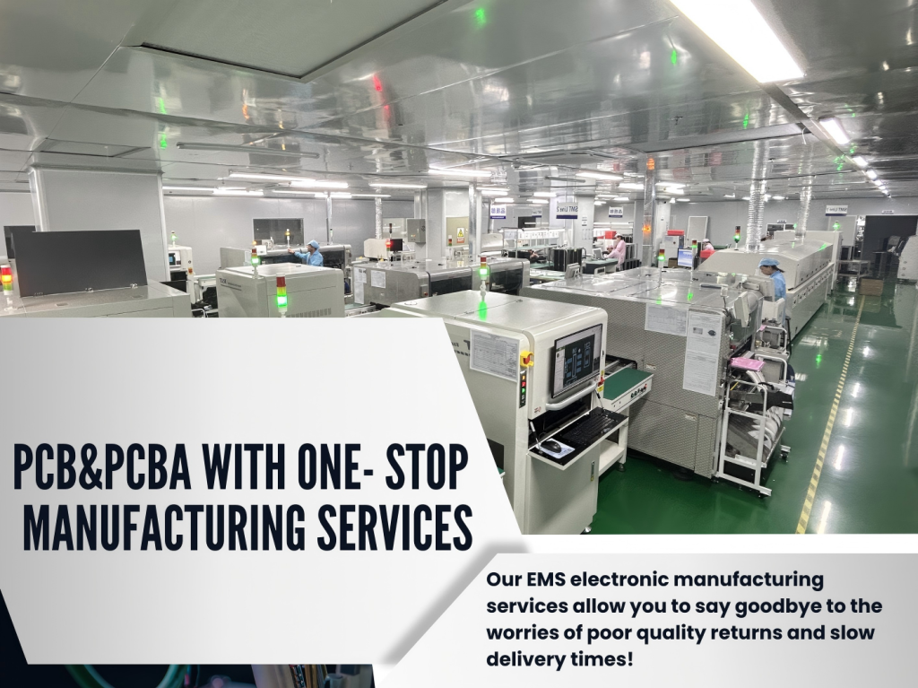
Hentech’s manufacturing facility in Shenzhen, Guangdong Province, China, is certified to an ISO 9001 quality management system, which allows us to implement strict quality control in all aspects of our operations. ISO 9001 certification provides significant support for our PCB testing and automated optical inspection services, which effectively reduces the risk of defects that are commonplace in the manufacturing process.
ISO 9001 relies on a set of quantifiable, flexible and scalable processes that are continuously optimized and refined as our business and that of our customers evolve. It is a central tool for ensuring accountability and transparency in the process, guaranteeing that all PCB testing is carried out in accordance with industry standards and using well-maintained, calibrated equipment.
Quick Request a Quote Form
We are happy to integrate inspection and test services into our PCB manufacturing processes, or as an essential part of turnkey manufacturing and contract manufacturing solutions. Every project starts with a comprehensive consultation, where our engineers will take a detailed look at your manufacturing and testing needs and provide you with a detailed quotation on how we can help you achieve your goals.
To initiate a partnership, please contact our head office via our online channel.

Sed ut perspiciatis unde omnis iste natus delavirot voluptatem accusantium doloremque laudanti totam aperiam inventore veritatis congueu. Olutpat elit nec nisi congue tristique eu at velit.
Phone
+86 137 9821 9394
Sale@hengele.com
Location
Room A, 3/F, Block 28, Chentian Industrial Area, Baotian 2nd Road, Xixiang Town, Bao'an District, Shenzhen, China
Customer Service
Subscribe Newsletter
Sed ut perspiciatis unde omnis iste natus feria delavirot.