
In the electronics manufacturing services industry, many companies provide design and engineering quotes that often require detailed technical information and specifications from the customer. However, this process is often complex and inconvenient for the customer.
Electronic Manufacturing Services is committed to simplifying this process. Simply tell us what you want to accomplish, and our team of engineers will take full responsibility for the subsequent design and assembly work, helping you complete your PCB project with ease.
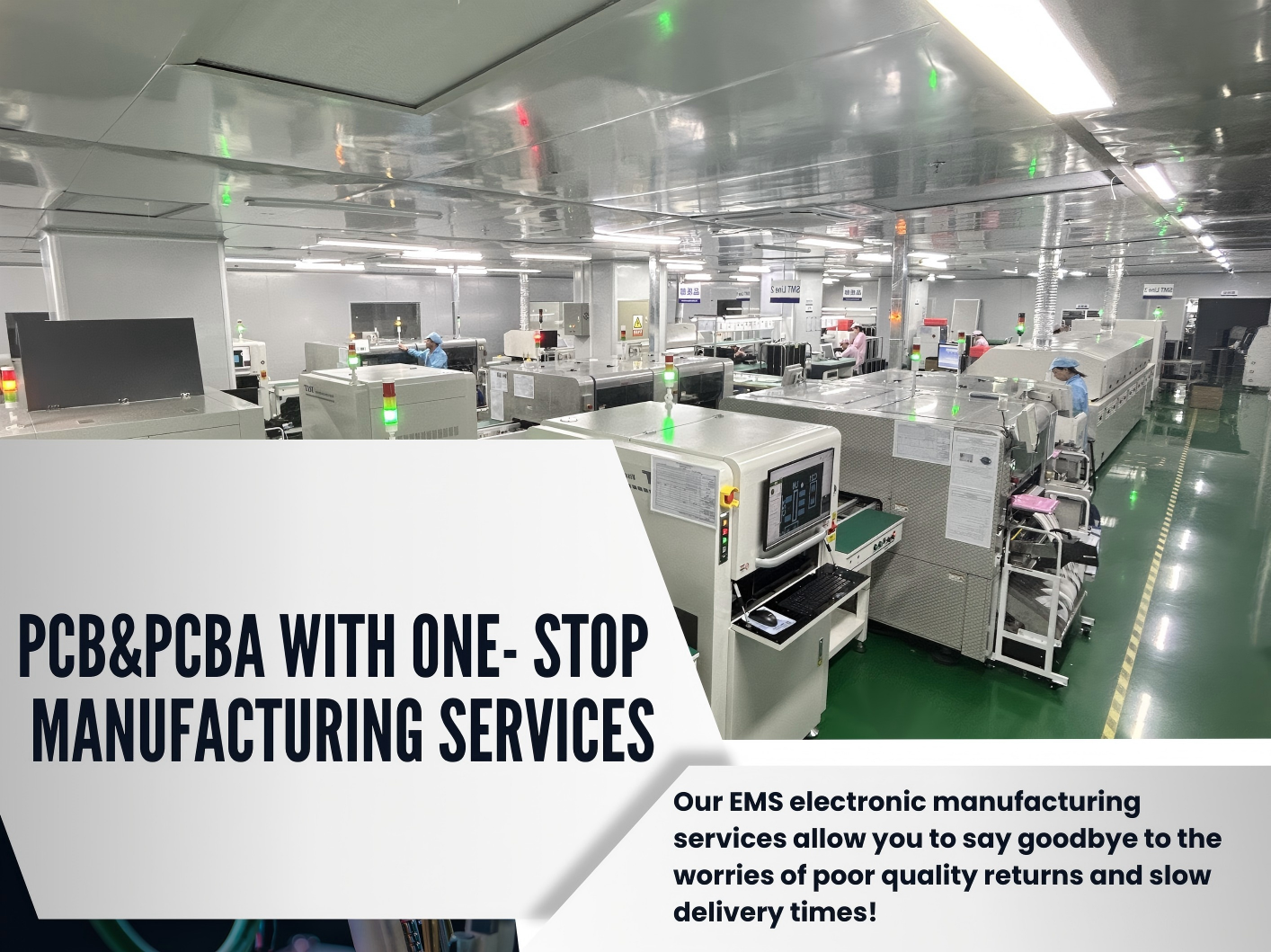
Hentech Specializes in PCB Design Excellence
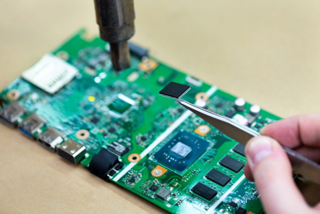
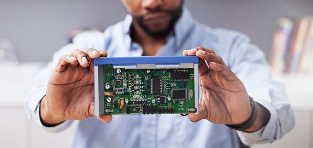
Hentech is a comprehensive PCB assembly solutions company with over 15 years of experience specializing in the assembly of printed circuit boards and electronic components. We are able to create customized design solutions to meet the unique requirements of different applications based on the specific needs of our customers. For example, our proprietary PCBs for data centers are designed to support the latest IoT technologies, helping to improve system efficiency and simplify the overall integration process.
PCB Layout Services Overview
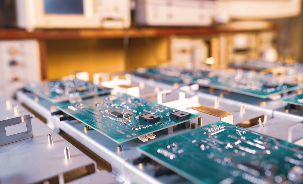
Printed Circuit Board (PCB) is an indispensable basic component in all electronic devices and is known as the “mother of all electronic products”. Through the conductive wiring on the PCB, different electronic components can be tightly integrated to accomplish the tasks of signal transmission and power supply, thus realizing the overall function of the device. Nowadays, PCBs are widely used in information technology, communication equipment, consumer electronics, automotive electronics, aerospace and military, precision instruments and various industrial equipment.
The main flow of PCB layout design is as follows:
◕ Component Construction
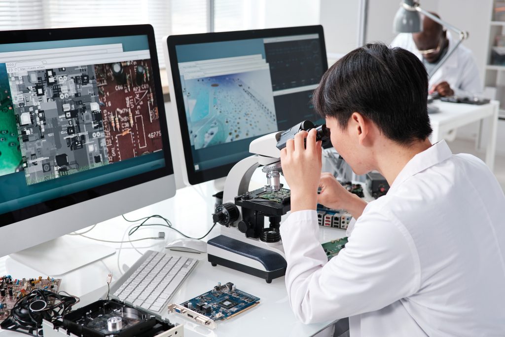
Although the company already has a complete component database, brand new parts often need to be imported into new projects. Engineers need to build components according to MTK part specifications and original factory datasheets, and then conduct rigorous audits after building, and finally incorporated into the system database for subsequent use.
◕ Pre-design planning and communication
Before entering the design stage, we need to fully communicate with the system analysis (SA), research and development (RD) and hardware engineering (HW) teams. Discussions include design criteria, PCB materials and processes, mechanism configurations, critical signal paths, impedance design, and functional verification requirements.
◕ Component Placement and Preliminary Design
The first step in circuit design begins with component placement, which directly affects subsequent routing, heat dissipation, and overall performance. This stage requires consideration of various factors such as high-frequency interference, electromagnetic compatibility, and mechanical constraints, and is a critical step in ensuring design quality.
◕ Circuit Wiring Design
After completing the component placement, the wiring work begins. Special signals (e.g., high-speed data lines, high-frequency lines) are prioritized and special attention is paid to line width, line spacing, and alignment length, which are usually required to be less than 0.1mm to ensure signal integrity and transmission efficiency. In addition, power supply and general signal routing are also designed according to standardized sequences. For high-end designs, simulations and optimizations are performed in collaboration with the high-frequency and EMC teams to achieve the goals of low interference, low latency, and impedance consistency.
◕ After the final review and output of the manufacturing data
circuit layout is completed, we work with the SA, RD, and HW teams again to confirm that the functionality is fully compliant with the original design intent. Then, we follow the MTK specification to ensure that all the design details are up to standard, and finally export the layout file in the manufacturer’s specified format to formally complete the entire PCB design process.
If you need assistance or want to know more about our PCB design and layout services, please feel free to contact us and we will try our best to provide you with the best solution.
Quick Request a Quote Form
Ready to get started? Get in touch today to learn more about our surface mount circuit board assembly services and book a consultation at your convenience by filling out our request a quote form. If you don’t have design or Gerber files we’ll work with you to create a design. If you require a quick turnaround PCB quote or lead time, please let us know and we’ll work with you to accommodate your specific needs.

Sed ut perspiciatis unde omnis iste natus delavirot voluptatem accusantium doloremque laudanti totam aperiam inventore veritatis congueu. Olutpat elit nec nisi congue tristique eu at velit.
Phone
+86 137 9821 9394
Sale@hengele.com
Location
Room A, 3/F, Block 28, Chentian Industrial Area, Baotian 2nd Road, Xixiang Town, Bao'an District, Shenzhen, China
Customer Service
Subscribe Newsletter
Sed ut perspiciatis unde omnis iste natus feria delavirot.