
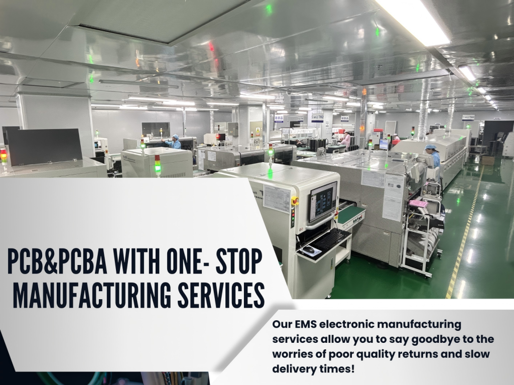
Our Facilities
We have a modern 3,500 m2 factory, of which 500 m2 is dedicated to office and engineering areas. Through scientific zoning and rationalization, we provide our customers with an efficient and reliable electronics manufacturing environment.
Office Systems and Resources
Our office areas are equipped with advanced computer network systems, inventory control, production scheduling, cost management, sales and invoicing, bill of materials, accounting and purchasing, and other key functions to ensure a high degree of synergy between information flow and production processes.
PCB Prototyping and Customized Development
Our engineering team is fully equipped to support the customization needs of high-precision products such as medical devices. While high-volume production can automate the component mounting process, we are equally adept at low-volume, highly complex circuit board assembly, paying particular attention to every detail to ensure that we meet our customers’ exclusive technical requirements.
We use specialized PCB design software to precisely control the layout and mounting position of each component for high-quality and efficient prototyping. Once prototyping is complete, we can quickly move on to the subsequent PCB assembly stage, shortening the time-to-market and improving overall project efficiency.
Surface Mount Components
Category: Single-arm, single-head high-speed applicator (click-to-change head, no downtime)
Applicator speed: 46,000 CPH (chips per hour, under optimal conditions)
Head type compatibility:
HM 10 suction nozzle head 46,000 CPH
HM 5 suction nozzle head 31,000 CPH (economical solution)
PCB size: 50 x 50mm to 510 x 460mm (optional L950mm version) Component size range: min. (optional L950mm version)
Component size range:
Minimum mounting: 0201 (0.2×0.1mm) / 03015 (0.3×0.15mm)
Maximum mounting: 55×100mm, up to 15mm
Height recognition: Multi-camera compatible, height >6.5mm or edge length >12mm with multi-camera support
Mounting accuracy: ±0.035mm (Cpk=1.0 at 3σ), Limit ±0.025mm
Component type: up to 96 types of tape racks (8 mm tape), 15 types of trays (with sATS15 option)
Placement speed: Dual beam structure with dual high-speed multi-purpose head (HM), up to 95,000 CPH (Chip Per Hour)
Placement head and component support:
HM (High-speed Multi-purpose) placement head: supports miniature components (e.g., 0201) up to 55×100mm, up to 15mm; wide scanning camera recognizes component sizes up to 12×12mm. 15mm; wide scanning camera recognizes component sizes up to 12×12mm
FM (Flexible Multi-Purpose) Placement Head: Supports non-standard component sizes from 30×15mm to 55×100mm, height ≤ 28mm
One Head for Multiple Components: The HM head can cover more than 90% of the common components without the need to change the head
Placement Accuracy and Recognition System:
Accuracy: ±0.035mm (3σ, Cpk ≥ 1.0), with limits to ±1.0mm. (3σ, Cpk ≥ 1.0), limit up to ±0.025mm
Intelligent Recognition: Equipped with wide scanning and side-view camera, realizing Flying Recognition without recognition time loss
Handles PCB sizes:
Single-track: 50×50mm to 810×490mm
Dual-track configuration, single-board same as the top or two boards up to a total of 810×662mm in width
Fixed Feeder Positions: Max. 140 *8mm tape
Trolley Feeder Position: 128 trolleys to support quick changeover
Pallet Options: Support for sATS30 system 30 pallets (stationary) or cATS10 10 pallets (cart)
Auto Loading Feeder (ALF): No interruption to tape changeover for improved productivity
Applicable stencil size: 370×470mm to 737×737mm; thickness 25-40mm
Applicable PCB size: 50×50mm to 400×340mm, support board thickness 0.4-6mm, FPC (fixture required) thickness ≤0.6mm
Pallet warping tolerance: ≤1%
Transportation height: 900 ± 40mm, support left/right direction bidirectional transport
Maximum transport speed: 1500mm/s (programmable)
Repeat positioning accuracy: ± 0.01mm
Printing accuracy: ± 0.025mm
A high-precision device specialized in solder paste quality control, widely used in SMT (surface mount technology) production lines. It ensures the accuracy of the height, width and thickness of the solder paste by means of advanced 3D inspection technology, thus improving solder quality and reducing production defects.
Main applications: Detection of under-tinning, missed prints, continuous tinning, over-tinning, misalignments, bad shapes, board contamination
Measuring principle: Digital structured grating phase modulation contouring technology
Pixels: 5M/12M
Reflow soldering equipment is designed for SMT electronic assembly, with high-precision temperature control and flexible configuration capabilities. Its core parameters include: temperature profile setting (lead-free soldering, for example) covers the preheating zone (room temperature to 150 ℃, the slope of the temperature ≤ 2 ℃ / s), constant temperature zone (150-180 ℃, 60-90 seconds), reflow zone (peak 235-245 ℃, lasting 10-20 seconds) and cooling zone (cooling rate of 3-5 ℃ / s); transfer speed adjustable range of 0.1-1.5m/min, recommended 0.8m/min suitable for most PCB boards; heating zone configuration 8 independent temperature zones, temperature control accuracy and flexible configuration capabilities. Recommended 0.8m/min suitable for most PCB boards; heating zone configuration of eight independent temperature zones, temperature control accuracy ± 1 ℃, total power 20kW.
optimization recommendations, including for high-density boards to reduce the transfer speed to 0.6m/min, heat-sensitive components to control the peak temperature of 230 ℃ or less, and regular maintenance of the chain and temperature sensors. The equipment is suitable for production in multiple scenarios from consumer electronics to automotive electronics, and the parameters need to be adjusted in accordance with product characteristics to ensure stability.
Production Equipment
This is an advanced automatic rework equipment, widely used in SMT (surface mount technology) production lines in the electronics manufacturing industry, mainly used for PCB soldering defects repair, especially for SMD (SMD) and BGA (ball grid array) components rework. The equipment is able to realize automatic alignment and accurate repair by means of a high-precision optical alignment system, which greatly improves the efficiency and precision of rework.
High-performance wave soldering equipment, widely used in the field of electronic product manufacturing, especially in the SMT (surface mount technology) production line, is mainly used to fix electronic components on the PCB board through welding.
Suitable for multi-industry coating application, multi-paneling, high capacity demand, and large area selective coating process with various manufacturing processes.
Various valve configurations and valve arrangements to meet the needs of various panelizing production.
The equipment is equipped with a spraying effect detection function, which can manually check the spraying quality in real time.
Testing and Inspection
It is widely used in electronic manufacturing industry, especially in SMT production line for First Article Inspection (FAI). It can automatically detect the quality of electronic products to ensure that each batch on the production line meets the standard, and improve production efficiency and quality through fast and accurate inspection.
High-precision and high-efficiency automatic optical inspection equipment, specialized in quality control in the electronics manufacturing industry, is mainly used for offline inspection of soldering defects, component mounting, pin alignment, etc., after the surface mount (SMT) production line of PCB boards.
The equipment, with its high-resolution optical system and intelligent software, enables comprehensive product inspection, improves product consistency and quality, and reduces defect rates.
In-line AOI (Automatic Optical Inspection) equipment designed specifically for SMT production lines. It is capable of monitoring the quality of PCBs in real time during the production process to ensure the soldering quality of each component, the correctness of component mounting and other surface defects, providing an efficient means of quality control.
X-ray inspection system, widely used in the electronics manufacturing industry, especially for lead-free soldering, BGA, QFN, CSP and other surface-mounted components (SMT) and package internal quality inspection. x1800 adopts advanced X-ray imaging technology, can accurately detect soldering defects, air holes, cracks, breaks, and other defects inside the PCB boards that are hidden under the appearance, so as to improve production quality and reduce rework rates.
Various oscilloscopes, meters and support equipment.

Quick Request a Quote Form
Ready to get started? Get in touch today to learn more about our surface mount circuit board assembly services and book a consultation at your convenience by filling out our request a quote form. If you don’t have design or Gerber files we’ll work with you to create a design. If you require a quick turnaround PCB quote or lead time, please let us know and we’ll work with you to accommodate your specific needs.

Sed ut perspiciatis unde omnis iste natus delavirot voluptatem accusantium doloremque laudanti totam aperiam inventore veritatis congueu. Olutpat elit nec nisi congue tristique eu at velit.
Phone
+86 137 9821 9394
Sale@hengele.com
Location
Room A, 3/F, Block 28, Chentian Industrial Area, Baotian 2nd Road, Xixiang Town, Bao'an District, Shenzhen, China
Customer Service
Subscribe Newsletter
Sed ut perspiciatis unde omnis iste natus feria delavirot.